
NTB5605T4G
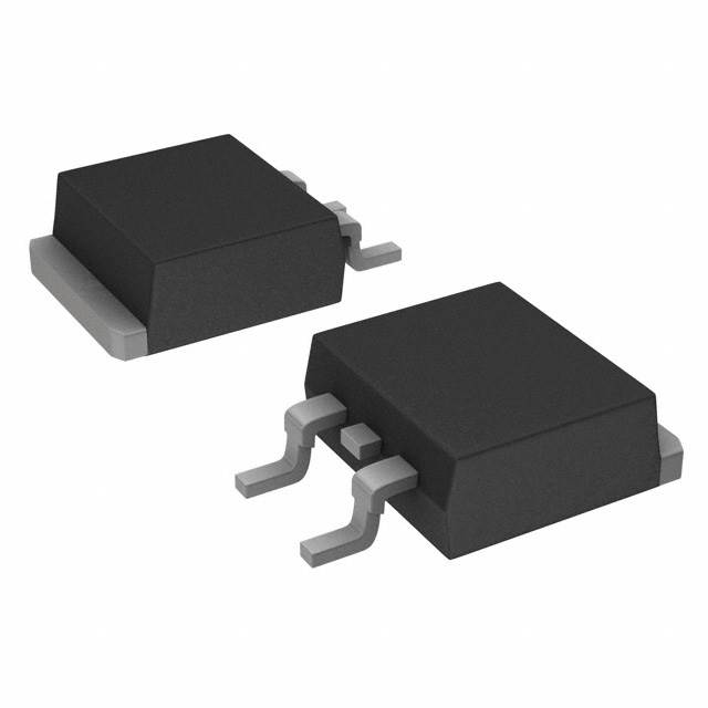
MOSFET P-CH 60V 18.5A D2PAKManufacturer: onsemi
Categories: Single FETs, MOSFETs
Quality Control: Learn More
onsemi's NTB5605T4G is a P-Channel MOSFET designed for power switching applications. This component features a Drain-to-Source Voltage (Vdss) of 60 V and a continuous Drain current (Id) capability of 18.5 A at 25°C (Ta). The device offers a maximum On-Resistance (Rds On) of 140 mOhms at 8.5 A and a gate drive voltage of 5 V. With a maximum power dissipation of 88 W (Tc), it is suitable for demanding thermal environments. Key parameters include a gate charge (Qg) of 22 nC and input capacitance (Ciss) of 1190 pF at 25 V, both measured at 5 V gate drive. The NTB5605T4G is housed in a TO-263-3, D2PAK (2 Leads + Tab) surface mount package, supplied in Tape & Reel (TR) for automated assembly. This MOSFET is utilized in industries such as automotive and industrial power control.
Additional Information
Series: -RoHS Status: unknownManufacturer Lead Time: No lead time information availableProduct Status: ObsoletePackaging: Tape & Reel (TR)Datasheet:Download Free CAD Model:
Technical Details:
| Packaging | Tape & Reel (TR) |
| Package / Case | TO-263-3, D2PAK (2 Leads + Tab), TO-263AB |
| Mounting Type | Surface Mount |
| Operating Temperature | -55°C ~ 175°C (TJ) |
| Technology | MOSFET (Metal Oxide) |
| FET Type | P-Channel |
| Current - Continuous Drain (Id) @ 25°C | 18.5A (Ta) |
| Rds On (Max) @ Id, Vgs | 140mOhm @ 8.5A, 5V |
| FET Feature | - |
| Power Dissipation (Max) | 88W (Tc) |
| Vgs(th) (Max) @ Id | 2V @ 250µA |
| Supplier Device Package | D2PAK |
| Drive Voltage (Max Rds On, Min Rds On) | 5V |
| Vgs (Max) | ±20V |
| Drain to Source Voltage (Vdss) | 60 V |
| Gate Charge (Qg) (Max) @ Vgs | 22 nC @ 5 V |
| Input Capacitance (Ciss) (Max) @ Vds | 1190 pF @ 25 V |