
FDD6690A
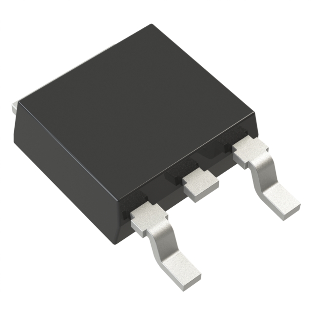
MOSFET N-CH 30V 12A/46A DPAKManufacturer: onsemi
Categories: Single FETs, MOSFETs
Quality Control: Learn More
The onsemi FDD6690A is an N-Channel PowerTrench® MOSFET featuring a 30V drain-source breakdown voltage. This device offers a continuous drain current of 12A at a temperature of 25°C (ambient) and 46A at 25°C (case). Its low on-resistance is specified at 12mOhm maximum at 12A and 10V Vgs. The FDD6690A supports gate drive voltages from 4.5V to 10V, with a maximum gate-source voltage of ±20V. Key parameters include a gate charge of 18 nC maximum at 5V and an input capacitance of 1230 pF maximum at 15V. Maximum power dissipation is 3.3W (ambient) and 56W (case). This MOSFET is housed in a TO-252AA (DPAK) surface mount package, suitable for applications in automotive and industrial power management. The operating junction temperature range is -55°C to 175°C.
Additional Information
Series: PowerTrench®RoHS Status: ROHS3 CompliantManufacturer Lead Time: No lead time information availableProduct Status: ObsoletePackaging: Tape & Reel (TR)Datasheet:Technical Details:
| Packaging | Tape & Reel (TR) |
| Package / Case | TO-252-3, DPAK (2 Leads + Tab), SC-63 |
| Mounting Type | Surface Mount |
| Operating Temperature | -55°C ~ 175°C (TJ) |
| Technology | MOSFET (Metal Oxide) |
| FET Type | N-Channel |
| Current - Continuous Drain (Id) @ 25°C | 12A (Ta), 46A (Tc) |
| Rds On (Max) @ Id, Vgs | 12mOhm @ 12A, 10V |
| FET Feature | - |
| Power Dissipation (Max) | 3.3W (Ta), 56W (Tc) |
| Vgs(th) (Max) @ Id | 3V @ 250µA |
| Supplier Device Package | TO-252AA |
| Drive Voltage (Max Rds On, Min Rds On) | 4.5V, 10V |
| Vgs (Max) | ±20V |
| Drain to Source Voltage (Vdss) | 30 V |
| Gate Charge (Qg) (Max) @ Vgs | 18 nC @ 5 V |
| Input Capacitance (Ciss) (Max) @ Vds | 1230 pF @ 15 V |