World’s First Functional 2D Microchip: KAUST Unveils a New Era in Microelectronics

More from the Category
A new era in microelectronics begins with a groundbreaking achievement at KAUST: the successful integration of atomically thin two-dimensional materials into a functional microchip. This milestone showcases the enormous potential of these exotic materials to enhance the performance and capabilities of microchip-based technologies.
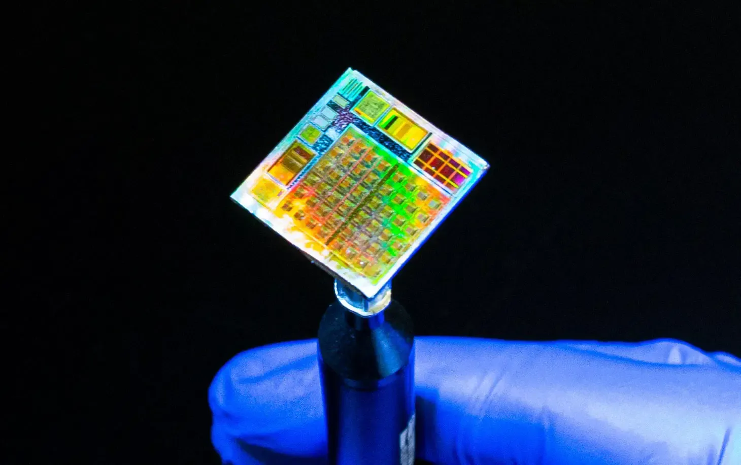
KAUST Professor Mario Lanza and his team have designed the world's first 2D microchip using synthetic materials. The chip functions as a high-performance, low-power neural network element, advancing microchip technology. KAUST, Mario Lanza
Since the discovery of graphene, an atomically thin layer of graphite, in 2004, there has been significant interest in utilizing similar materials for innovative and advanced applications due to their extraordinary physical properties. However, despite two decades of research, developing functional microdevices using these two-dimensional materials has been challenging due to the delicate nature of thin films and the difficulties associated with their fabrication and handling.
Inspired by recent breakthroughs in Professor Lanza’s laboratory involving functional two-dimensional films, a collaborative effort led by KAUST has successfully produced and demonstrated a prototype microchip based on these materials.
“Our goal was to advance the technology readiness level of electronic devices and circuits based on two-dimensional materials by using conventional silicon-based CMOS microcircuits as a foundation and employing standard semiconductor fabrication techniques,” explains Lanza. “However, we faced challenges, such as potential defects like atomic impurities present in synthetic two-dimensional materials, which can cause small devices to fail. Additionally, integrating the 2D material into the microchip without causing damage proved to be extremely difficult.”
To overcome these challenges, the research team optimized the chip’s design to simplify fabrication and minimize the impact of defects. They achieved this by fabricating standard complementary metal-oxide-semiconductor (CMOS) transistors on one side of the chip and routing interconnects to the underside, where the 2D material could be reliably transferred onto small pads measuring less than 0.25 micrometers.
“We synthesized hexagonal boron nitride (h-BN), a two-dimensional material, on copper foil and then used a low-temperature wet process to transfer it onto the microchip. Subsequently, we applied conventional vacuum evaporation and photolithography techniques available in our facility to form electrodes on top,” elaborates Lanza. “In this way, we created a 5×5 array of one-transistor/one-memristor cells interconnected in a crossbar matrix.”
The unique properties of the 18-atom thick h-BN, equivalent to 6 nanometers, make it an ideal memristor—a resistive component with adjustable resistance based on the applied voltage. Each microscale memristor pad in the 5×5 configuration is linked to a dedicated transistor, enabling precise voltage control for the memristor to function effectively with high performance and reliability over numerous cycles. In this case, the microchip serves as a low-power neural network element.
“Following this groundbreaking achievement, we are in discussions with leading semiconductor companies to continue our progress in this field,” reveals Lanza. “Additionally, we are considering the installation of our own large-scale industrial processing system for 2D materials at KAUST to further enhance this capability.”
Learn more at SciTechDaily.