Laser Photonics Expands Semiconductor Industry-Focused Product Line

More from the Category
Laser Photonics Corporation, a leader in industrial laser technologies, is making waves in the semiconductor industry with its latest product line expansion. As global demand for semiconductors continues to skyrocket — driven by advancements in electronics, electric vehicles, and artificial intelligence — the need for precision and efficiency in chip manufacturing has never been greater.
Semiconductor fabrication is a complex process requiring innovative solutions to meet the growing demand for high-performance chips. Laser Photonics’ advanced systems address critical challenges faced by manufacturers by enhancing efficiency and precision.
This article explores Laser Photonics’ expanded product offerings, their strategic importance in semiconductor production, and the broader implications for the semiconductor industry.
The Growing Need for Advanced Semiconductor Solutions
The semiconductor industry is experiencing unprecedented growth, fueled by innovations in consumer electronics, electric vehicles (EVs), industrial automation, and artificial intelligence (AI). Analysts project that the global semiconductor market could reach an astonishing $1 trillion annually by 2030. This rapid expansion underscores the critical role semiconductors play in powering the technologies that define modern life.
However, this growth comes with significant challenges. The semiconductor supply chain, still recovering from pandemic-induced disruptions, is struggling to meet surging demand. Chip shortages have highlighted vulnerabilities in global production systems and pushed manufacturers to seek more efficient and reliable fabrication methods. At the same time, as chips become smaller and more complex, the precision required in manufacturing processes has increased dramatically.
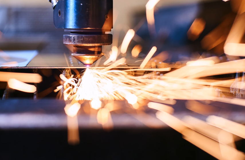
High-speed laser technologies, such as those offered by Laser Photonics, are emerging as indispensable tools in this landscape. Processes like laser wafer dicing and laser wafer marking provide manufacturers with the precision and scalability needed to handle complex chip designs and high production volumes. Unlike traditional methods that rely on mechanical tools or chemical processes, laser-based solutions are faster, cleaner, and more adaptable to the intricate demands of modern chip fabrication.
The demand for advanced solutions extends beyond production efficiency. Industries reliant on semiconductors require chips with higher performance, lower defect rates, and enhanced traceability. This need for precision and quality assurance has pushed semiconductor manufacturers to adopt cutting-edge technologies that minimize waste and maximize yields. Laser Photonics’ expanded product line directly addresses these needs to help manufacturers stay competitive.
Highlighting Laser Photonics’ New Offerings
Laser Photonics has stepped up to meet the semiconductor industry’s growing demands with an expanded product line tailored to improve efficiency and precision in chip manufacturing. The company’s innovative technologies target critical areas of semiconductor production and offer solutions that enhance performance while addressing common challenges.
BlackStar Laser Wafer Dicing System
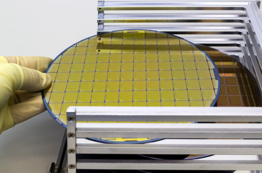
At the center of Laser Photonics’ new lineup is the BlackStar Laser Wafer Dicing System, a cutting-edge tool designed to streamline the wafer dicing process. This system employs short-pulse laser technology to achieve exceptional precision in die singulation. Unlike traditional mechanical dicing methods, which generate heat and require water jet cooling, the BlackStar system operates with minimal heat generation and eliminates the need for water cooling. This makes it particularly effective for dicing brittle materials like silicon and sapphire.
The BlackStar system delivers several key benefits:
● Higher Yield: By minimizing material stress and damage, it significantly reduces wafer breakage and boosts overall chip yield.
● Faster Processing: Its high-speed operation saves time, allowing manufacturers to keep up with production demands.
● Cost Efficiency: Reduced labor and maintenance make it a more cost-effective solution for chipmakers.
Comprehensive Multi-Station Laser Systems
In addition to the BlackStar system, Laser Photonics has introduced multi-station laser platforms that address a range of semiconductor fabrication tasks. These systems integrate robotic wafer positioning and machine vision to enable precision wafer marking, scribing, and lapping. By automating these processes, manufacturers can improve throughput and maintain consistency in high-volume production environments.
Advanced Laser Wafer Marking Technology
Marking and traceability are critical in semiconductor manufacturing to ensure quality control and tracking throughout the production cycle. Laser Photonics’ laser wafer marking systems leverage ultraviolet (UV) laser technology to create permanent, detailed markings without compromising the structural integrity of the wafer. This is particularly important for chips used in high-performance applications, where even minor surface damage can affect functionality.
Innovations in Laser Wafer Dicing Technology
Laser wafer dicing has emerged as a transformative technology in semiconductor manufacturing. Traditional wafer dicing methods, which rely on mechanical saws or chemical etching, often face limitations in accuracy, scalability, and material compatibility. Laser Photonics’ advancements in laser wafer dicing technology are redefining the standards for this critical process.
Precision Without Compromise
The cornerstone of laser wafer dicing technology is its ability to achieve high precision without causing thermal or mechanical stress on the wafer. Laser Photonics’ BlackStar Laser Wafer Dicing System utilizes short-pulse lasers that produce minimal heat during operation, which eliminates the need for water jet cooling. This innovation not only simplifies the process but also ensures that the delicate microstructures of modern semiconductor wafers remain intact.
This level of precision is particularly crucial for working with brittle materials like silicon, gallium arsenide, and sapphire, which are prone to cracking and chipping when handled with traditional methods. The result is a higher yield of usable dies, which directly impacts production efficiency and cost-effectiveness.
Faster, Cleaner, Smarter
Speed and cleanliness are critical in semiconductor manufacturing, where even microscopic contamination can lead to defects. Laser wafer dicing systems significantly outperform mechanical dicing tools in both aspects. By using a non-contact method, lasers eliminate debris and particulate contamination common in traditional cutting processes. Additionally, the high-speed operation of Laser Photonics’ systems allows manufacturers to process more wafers in less time.
Smart features like machine vision and robotic positioning that are integrated into Laser Photonics’ systems further enhance the dicing process. These technologies enable precise alignment and cutting to ensure consistency and reduce human error. The automation also seamlessly integrates into high-volume production lines to improve overall throughput.
Environmental and Cost Benefits
Laser wafer dicing technology offers environmental and cost advantages that are increasingly important in today’s semiconductor market. The elimination of water cooling reduces resource consumption and minimizes waste. Additionally, the high efficiency and reduced waste lower operational costs, which makes laser dicing a more sustainable and economical option for manufacturers.
Laser Photonics’ innovations in laser wafer dicing technology are setting new benchmarks for efficiency, accuracy, and sustainability in semiconductor fabrication.
Strategic Expansion and Acquisition
Laser Photonics’ recent expansion of its semiconductor-focused product line is a strategic move underpinned by the company’s acquisition of Control Micro Systems (CMS). This acquisition has significantly bolstered Laser Photonics’ technical capabilities and market positioning, allowing it to cater more effectively to the semiconductor industry’s evolving needs.
Enhancing Capabilities Through CMS
Control Micro Systems, a renowned provider of laser-based manufacturing solutions, brings decades of expertise to Laser Photonics. By integrating CMS’s technology and knowledge base, Laser Photonics has accelerated its ability to deliver advanced and customizable solutions for semiconductor manufacturers. This synergy resulted in the development of the BlackStar Laser Wafer Dicing System, which combines CMS’s precision engineering and Laser Photonics’ cutting-edge laser technology.
Expanding Product Portfolio
The acquisition has enabled Laser Photonics to diversify its offerings and introduce multi-station systems that address critical aspects of semiconductor production beyond wafer dicing. These include solutions for wafer marking, scribing, and lapping, all of which are enhanced by CMS’s robotics and automation expertise. This expanded product line reflects the company’s commitment to providing end-to-end solutions that streamline semiconductor manufacturing.
Driving Industry Leadership
Laser Photonics CEO, Wayne Tupuola, has emphasized the strategic importance of the CMS acquisition, stating,
“Our growth is fueled by the addition of CMS, and we are excited to expand our product portfolio and offer high-speed, effective laser equipment to chip fabs.”
This forward-thinking approach not only strengthens the company’s market presence but also positions it as a key innovator in the semiconductor sector.
Scaling for Future Growth
The CMS acquisition also aligns with Laser Photonics’ broader vision of scaling its operations to meet the increasing global demand for semiconductors. By combining resources and expertise, the company is better equipped to address the challenges of an industry characterized by rapid technological advancements and heightened competition.
Laser Photonics’ strategic expansion through the acquisition of Control Micro Systems demonstrates its commitment to driving innovation and delivering value to semiconductor manufacturers. This move has not only enhanced its product capabilities but also reinforced its position as a leader in the highly competitive semiconductor technology market.
Industry Implications
Laser Photonics’ advancements in semiconductor-focused laser technologies come at a pivotal time for the industry. As global demand for high-performance semiconductors accelerates, manufacturers are under immense pressure to improve production efficiency, enhance precision, and maintain competitiveness. The company’s innovations in laser wafer dicing, marking, and automation address some of the most pressing challenges in chip fabrication.
The introduction of the BlackStar Laser Wafer Dicing System and multi-station laser platforms provides manufacturers with tools to optimize yield and reduce waste. By minimizing wafer damage and ensuring clean, precise cuts, these technologies improve die output while lowering production costs. Such advancements are especially critical for handling brittle materials like silicon and sapphire, which are central to modern chip designs.
Automation features, such as robotic wafer positioning and machine vision, not only increase production speed but also reduce dependency on skilled labor, which is often a bottleneck in semiconductor manufacturing. Additionally, the integration of ultraviolet laser marking systems ensures traceability without compromising chip quality, a growing necessity as semiconductors power more critical applications in automotive, aerospace, and healthcare.
Beyond technical benefits, these innovations enhance the industry’s ability to scale. With demand continuing to increase exponentially, tools like Laser Photonics’ systems will play a vital role in meeting global needs while maintaining quality standards. By addressing efficiency, precision, and scalability, Laser Photonics is helping reshape the future of semiconductor production and set new benchmarks for the industry.
Sourcing Semiconductors
Just as Laser Photonics is setting new standards for manufacturing semiconductors, Microchip USA is raising the bar in supplying them. With a team of veteran purchasing and supply chain specialists and industry-leading quality control, we add unparalleled value to all of our customers’ businesses. Whether you’re looking for a single board-level electronics component or a partner who can manage your entire supply chain, we’re here to help. Contact us today!