AMD Unveils Revolutionary VP1902

More from the Category
In a groundbreaking development, AMD has unleashed its latest innovation – the AMD VP1902, set to be the largest FPGA (Field-Programmable Gate Array) in the world. This colossal FPGA is specifically designed to emulate future silicon designs, ranging from small Systems on Chips (SoCs) like those found in Raspberry Pi devices to powerful next-generation accelerators like the AMD Instinct MI300.

The previous generation, Xilinx VU19P, held the crown as the largest FPGA upon its release. However, the VP1902 surpasses its predecessor by integrating Versal features and adopting a new chipset design from AMD. As a result, the key capabilities of these FPGAs are more than doubled.
For many years, Xilinx (now AMD) has dedicated a product line to facilitate the emulation and debugging of silicon. The common approach to chip design involves using tools to deploy logic onto a series of large FPGAs and emulate the design well before it undergoes silicon manufacturing. As chip complexity increases, the number of gates required also rises. While there is no precise gate-to-transistor ratio, experts approximate that around 4 transistors in silicon roughly equate to 1 gate on these FPGAs (though there are significant variabilities).
The AMD Versal Premium VP1902 redefines the gate count capabilities by effectively doubling the number of gates that can be emulated, with an impressive capacity of up to 18.5 million logic cells. Additionally, AMD enhances the FPGA with more transceivers and increased transceiver bandwidth, facilitating the connection of more devices and expanding the emulation capabilities. To provide context, these FPGAs can scale from a single device to over 1000 connected FPGAs, enabling the emulation of extensive silicon designs.
Apart from the expanded programmable logic cell count, AMD has introduced a range of unique features to the VP1902, which differentiates it from the AMD Xilinx VU19P. These features include:
- New Processing System
- Programmable Network on Chip (NoC)
- Hardened DDR Memory Controllers (14x)
- Four 600G Ethernet MACs (Supports 100-400G Ethernet, totaling 600G bandwidth)
- Twelve 100G Ethernet MACs (Supports 10-100G Ethernet)
In comparison to the VU19P, the VP1902 boasts 16x PCIe Gen5 x4 hard IP blocks, while the VU19P had 8x PCIe Gen4 x8. This upgrade results in a remarkable 36% lower latency scaling from chip to chip. Furthermore, the VP1902 features a significant clock speed boost. These advancements go beyond the mere increase in programmable logic cells, marking a significant step forward for the FPGA.
The additional IP integrated into the VP1902 means that fewer programmable logic cells are required to accommodate this IP, enabling more efficient utilization of the floorplan for emulation. AMD has also leveraged its NoC for debugging purposes and the restoration of designs to specific register states, greatly aiding the debugging process. This functionality is available without the need to develop it from scratch.
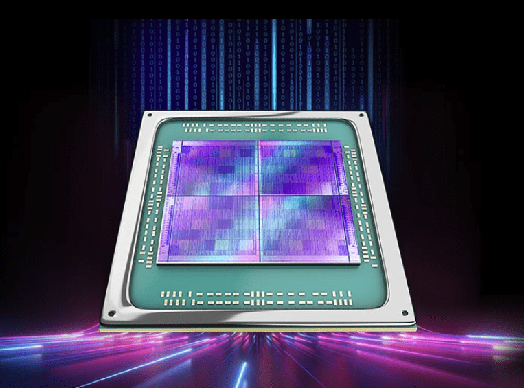
The AMD VP1902 represents a monumental achievement, showcasing AMD’s ingenuity and innovation. Notably, this extraordinary chip features two sets of mirrored and rotated dies (four in total) integrated into a single package. At first glance, one might mistake it for a 4th Gen Intel Xeon Scalable Sapphire Rapids, highlighting the impressive design and engineering of the VP1902.
Learn more at AMD, The Register, and HPCwire.