Ultimate Guide to High Bandwidth Memory

More from the Category
In today’s data-driven world, the growth of artificial intelligence (AI), cloud computing, and high-performance workloads has pushed traditional DRAM to its limits. As the need for faster data processing intensifies, a breakthrough technology has stepped in to meet these demands: High Bandwidth Memory (HBM).
HBM is the next-generation memory architecture that enables faster data transfer, improved energy efficiency, and compact integration - key to supporting everything from large language models to advanced graphics rendering.
In this article, we’ll explore what HBM is, how it works, its major applications, who manufactures it, the state of the high bandwidth memory market, and the innovations driving its future.
What Is HBM? The Architecture Behind High Bandwidth Memory
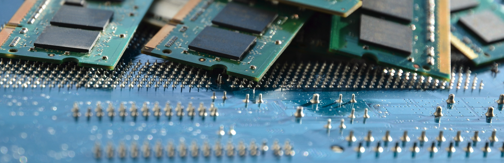
High Bandwidth Memory (HBM) is a high-performance 3D-stacked DRAM architecture connected through Through-Silicon Vias (TSVs) - vertical electrical connections that link multiple DRAM layers together. These stacks sit atop a silicon interposer, placed very close to the processor, reducing the distance data must travel and dramatically improving speed and efficiency.
Unlike conventional DDR or GDDR memory, HBM memory delivers massive parallel data bandwidth while consuming significantly less power. Its proximity to the processor allows it to support multi-terabyte-per-second throughput, ideal for data-intensive applications like AI training, HPC, and advanced graphics rendering.
Key Advantages of HBM
· Extremely high bandwidth
· Lower latency than DDR or GDDR
· Smaller physical footprint
· Reduced power consumption
In short, HBM isn’t just a faster form of memory - it’s a complete rethinking of how memory communicates with processors.
What Is High Bandwidth Memory Used For?
High Bandwidth Memory (HBM) is used in systems that demand rapid data transfer and low power consumption. As data complexity increases, HBM serves as a high-performance backbone for applications like AI training, data analytics, and high-end graphics processing.
Industry Transformation
AI and Deep Learning: HBM powers massive model training and inference workloads, supporting trillion-parameter models for large language systems like ChatGPT.
High-Performance Computing (HPC): Used in supercomputers and data analytics systems that rely on parallel processing for large-scale simulations.
Graphics and Gaming: Enables ultra-fast rendering for next-generation GPUs and gaming consoles.
Cloud and Data Centers: Boosts throughput in high-performance servers handling AI and analytics tasks.
Autonomous Vehicles and Networking: Supports edge computing, sensor fusion, and low-latency communications critical for decision-making in real time.
HBM is the memory technology enabling the current wave of intelligent computing.
Evolution and Types of HBM Memory
Since its introduction, HBM memory has undergone rapid evolution. Each generation improves performance, power efficiency, and integration flexibility.
· HBM1 (2015): Introduced the first 3D-stacked DRAM using TSVs, delivering around 128 GB/s bandwidth.
· HBM2 / HBM2E: Boosted speeds to 410–460 GB/s per stack, supporting 8-high layers.
· HBM3 / HBM3E: Achieved up to 4.8 TB/s of bandwidth and greater density for AI acceleration.
· HBM4 / HBM4E (Upcoming): Expected to exceed 1 TB/s per stack and introduce customizable base logic dies and 2,048-bit interfaces, doubling the data lines from HBM3.
Generational updates now occur every 2 - 2.5 years, far faster than traditional DRAM, as AI hardware development demands higher bandwidth and integration.
High Bandwidth Memory Manufacturers: Who Makes HBM?
The high bandwidth memory market is dominated by three global manufacturers - SK hynix, Samsung Electronics, and Micron Technology. These companies lead the industry in advanced packaging, custom HBM architectures, and collaborations with AI chipmakers like NVIDIA, AMD, and Broadcom.
Advanced Packaging and Customization
Modern HBM depends on 2.5D silicon interposers and Through-Silicon Vias (TSVs) to connect stacked DRAM dies to processors. Packaging companies like ASE report record demand as AI and networking applications push the limits of interconnect speed and reliability.
All three major manufacturers are now embracing custom HBM architectures, optimized for power, performance, and area (PPA), to align more closely with GPU and AI accelerator designs. Customization has become the key differentiator in the high-bandwidth memory market.
SK hynix: The HBM Pioneer
SK hynix pioneered the commercialization of HBM and continues to lead with first-to-market innovation. In 2025, it completed HBM4 development and began preparing for mass production. The company shipped 12-Hi HBM4 samples to major partners like NVIDIA, achieving data transfer speeds exceeding 2TB/s.
Built using TSMC’s 12nm logic process, SK hynix’s HBM4 sets the benchmark for bandwidth and energy efficiency. It employs a proprietary Mass Reflow Molded Underfill (MR-MUF) process, which enhances thermal conductivity and reliability across tall DRAM stacks.
SK hynix also plans to launch custom HBM4E products for clients such as NVIDIA, AMD, and Broadcom, tailoring architectures for specific AI workloads.
Samsung Electronics: Pushing the Limits with Custom and 3D Stacks
Samsung Electronics remains a fierce competitor in the high-bandwidth memory manufacturers’ landscape. In late 2025, Samsung shipped HBM4 samples with 11Gbps pin speeds, matching Micron’s performance records, and plans to begin mass production by the end of the year.
Samsung’s 12-layer HBM3E modules offer up to 1,280 GB/s bandwidth and 36 GB capacity while maintaining the same height as 8-layer stacks. Using Non-Conductive Film (NCF) and Thermocompression Bonding (TCB), Samsung ensures precision bonding and reduces defect risks in fine-pitch interconnects.
Looking forward, Samsung is developing 3D DRAM stacking - turning DRAM cells vertically like NAND flash - to reduce power and area consumption. Relocating the memory controller onto the base die will free up space for AI compute logic, creating tightly integrated and more efficient memory architectures.
Micron Technology: Redefining Performance and Efficiency
Micron Technology has made bold moves in the HBM memory race, achieving record-breaking performance with its 12-Hi HBM4 samples. Announced in early 2025, these modules surpass JEDEC’s HBM4 standards, offering 2.8TB/s bandwidth and 11Gbps pin speeds.
Micron’s success lies in its 1-gamma DRAM node and CMOS-based packaging innovations, combining high efficiency with scalable manufacturing. Partnering with TSMC, Micron has also co-developed HBM4E - a next-generation solution featuring customizable base logic dies for optimized latency and packet routing in AI accelerators from NVIDIA and AMD.
CEO Sanjay Mehrotra confirmed Micron’s HBM revenue is expected to exceed $8 billion in 2025, with HBM4E products delivering higher margins and increased market share in the competitive high bandwidth memory market.
Engineering Challenges and The Road Ahead
Despite remarkable advances, all high-bandwidth memory manufacturers face similar challenges:
· Managing TSV yield and thermal performance in tall memory stacks.
· Addressing warpage and mechanical stress during packaging.
· Reducing the high cost of silicon interposers and TSV fabrication.
The transition to hybrid bonding - which eliminates microbumps - is expected to improve density, efficiency, and long-term reliability in HBM4E and future generations.
Together, SK hynix, Samsung, and Micron are racing to dominate the $100 billion HBM4 market, each pushing the boundaries of speed, customization, and efficiency.
The High Bandwidth Memory Market: Growth, Trends, and Forecast
According to Bloomberg Intelligence (2025), the high bandwidth memory market is on a historic growth trajectory, projected to expand from $4 billion in 2023 to $130 billion by 2033 - a 42% compound annual growth rate (CAGR).
By 2033, HBM memory is expected to represent over 50% of the global DRAM market value and 10% of total industry bit shipments, driven primarily by AI computing and large-scale machine learning models.
Key Market Insights
AI Growth: As model sizes grow exponentially, AI chips demand more memory capacity per device, tightening supply and driving higher prices.
Next-Gen Launches: HBM4 and HBM4E releases (2025–2026) are forecast to increase prices by about 20% over HBM3E.
Market Leaders by 2033:
· SK hynix: 40%
· Samsung: 35%
· Micron: 23%
Capacity Expansion: Production capacity is expected to double annually (2023–2026), but oversupply is not anticipated before 2033 due to continuous AI demand.
The high bandwidth memory market will remain one of the fastest-growing segments in semiconductors through the next decade.
Challenges, Opportunities, and Innovation Cycles in HBM Memory
Challenges
While HBM enables breakthrough performance, it also presents significant engineering and economic challenges:
· Manufacturing complexity from TSV processing and wafer stacking.
· Thermal management for 12–16-high DRAM stacks.
· Yield optimization and defect mitigation at advanced nodes.
· Lagging standardization, as JEDEC’s 4–5-year update cycle trails the industry’s 2-year pace.
Opportunities
Despite these challenges, the opportunities are substantial:
· Growing demand for custom HBM memory in AI accelerators and cloud infrastructure.
· 3D packaging and hybrid bonding innovations improving scalability.
· Closer foundry collaboration, like Micron–TSMC, enabling integrated design optimization.
Innovation Outpacing Standards
The HBM innovation cycle has now surpassed formal standardization. GPUs evolve annually, and HBM generations shift every 2–2.5 years, compared to JEDEC’s slower cadence. Companies like Marvell, Micron, and SK hynix are developing custom HBM architectures that integrate logic, memory, and interconnects to achieve extreme bandwidth.
For many, customization now outweighs standardization - especially as hyperscalers and chipmakers prioritize performance over uniformity.
Companies Driving HBM Demand
The ecosystem driving HBM innovation spans across industries:
NVIDIA: The leading consumer of HBM memory, using it across GPUs and AI accelerators like the Blackwell series.
AMD and Intel: Integrating HBM into next-gen HPC and data-center processors.
Cloud Providers: Google, AWS, and Microsoft are developing in-house AI chips with integrated HBM stacks.
Automotive, Defense, and Telecom: Leveraging high bandwidth memory for real-time data processing, sensor fusion, and edge compute systems.
These companies collectively fuel the rapid expansion of the high-bandwidth memory market, ensuring continuous innovation and demand.
Powering the Next Generation of AI and High Performance Computing
The rise of High Bandwidth Memory (HBM) marks a defining moment in the semiconductor industry. It bridges the performance gap between processors and data, enabling the next era of AI, HPC, and intelligent systems.
However, as memory technology advances, sourcing older or discontinued components becomes increasingly challenging. That’s where Microchip USA can help.
If you’re looking for obsolete or hard-to-find memory, contact Microchip USA - Your trusted global distributor for reliable, high-quality semiconductor solutions.
More from the Category
Line Cards We Support