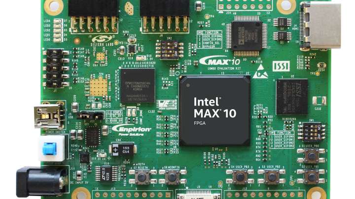
Altera’s MAX 10 FPGA

More from the Category


Introduction to MAX10 FPGA
The MAX10 FPGA is a high-performance, low-cost field-programmable gate array developed by Altera, which originally became part of Intel in 2015. In 2024, Altera was re-established as an independent company, with Intel retaining a minority stake. Today, MAX10 continues under the Altera brand, operating independently while collaborating closely with Intel Foundry Services.
Built on a flexible architecture inspired by the performance legacy of Arria 10, MAX10 strikes a balance between affordability and capability. Its versatile logic, embedded memory, DSPs, and high-speed transceivers make it an attractive platform for a wide range of embedded and high-throughput applications.
MAX10 FPGA Architecture
The MAX10 FPGA architecture is based on Arria 10 technology, known for its high performance and low power consumption. It consists of several key components:
• Scalable Logic Array: The MAX10 FPGA provides a scalable logic array that can accommodate up to 100,000 logic cells. These logic cells can be interconnected to implement complex digital designs efficiently.
• Embedded Memory Blocks: To enable efficient data storage and processing, the MAX10 FPGA includes embedded memory blocks. These blocks can provide up to 128MB of on-chip memory, allowing for high-speed access and manipulation of data.
• Digital Signal Processing (DSP) Blocks: DSP blocks are specialized components within the MAX10 FPGA that are optimized for performing high-speed arithmetic operations. These blocks are useful for implementing algorithms such as digital filters, signal processing, and mathematical computations.
• High-Speed Transceivers: The MAX10 FPGA supports high-speed transceivers, which enable fast data communication and interconnectivity. These transceivers can provide up to 100Gbps of bandwidth, making the MAX10 FPGA suitable for applications requiring high-speed data transfer.
MAX10 FPGA Features
The MAX10 FPGA offers several notable features that contribute to its versatility and performance:
• Logic Cells: The MAX10 FPGA supports up to 100,000 logic cells, providing ample resources for implementing complex digital designs. Logic cells are fundamental building blocks that can perform various logical operations, enabling the creation of intricate digital circuits.
• On-Chip Memory: The MAX10 FPGA includes embedded memory blocks, providing up to 128MB of on-chip memory. This on-chip memory allows for efficient data storage and processing, reducing the need for external memory components.
• Transceiver Bandwidth: High-speed transceivers are integrated into the MAX10 FPGA, offering up to 100Gbps of bandwidth. This feature enables the FPGA to handle high-speed data communication and interconnectivity, making it suitable for applications that require fast data transfer rates.
• DDR4 Memory Support: The MAX10 FPGA includes dedicated memory controllers that support DDR4 SDRAM. This support allows for efficient interfacing with DDR4 memory modules, enabling faster and more reliable memory access.
• I/O Interfaces: The MAX10 FPGA supports multiple I/O standards, including LVDS, LVCMOS, and SSTL. This flexibility enables seamless integration with various external devices and peripherals, making it easier to interface the FPGA with the rest of the system.
MAX10 FPGA Applications
The MAX10 FPGA finds applications in a diverse range of fields:
• Industrial Automation: The MAX10 FPGA can be used in industrial automation settings to implement real-time control systems, motor control, and communication interfaces. Its high-performance capabilities and flexibility make it well-suited for industrial applications that require precise control and data processing.
• Medical Devices: In the field of medical devices, the MAX10 FPGA provides a flexible platform for designing and implementing various systems. It can be used in applications such as patient monitoring systems, medical imaging equipment, and diagnostic instruments, where high-performance processing and real-time data analysis are crucial.
• Networking: The MAX10 FPGA is an excellent choice for networking applications that require high-bandwidth and low-latency data processing. It can be used to develop routers, switches, network interface cards (NICs), and other networking equipment. The FPGA’s ability to handle high-speed data communication and its support for various I/O standards make it ideal for networking applications.
• Consumer Electronics: The MAX10 FPGA is well-suited for consumer electronics products that demand high performance and customization. It can be used in applications such as high-definition displays, audio/video processing devices, smart home automation systems, and other consumer electronics where flexibility, speed, and power efficiency are essential.
• Test and Measurement: The MAX10 FPGA is also suitable for test and measurement applications. Its programmable nature allows for implementing signal processing algorithms, data acquisition, and instrument control. It can be utilized in test and measurement equipment, such as oscilloscopes, spectrum analyzers, and data loggers.
MAX10 FPGA Programming
MAX10 FPGAs are programmed using tools developed by Altera, now offered under the standalone Altera brand with legacy support from Intel. The core software suite remains Quartus Prime, which supports design entry, synthesis, implementation, and device programming.
Programming Process:
• Design Entry: Describe the digital design using a hardware description language (HDL) such as VHDL or Verilog.
• Compilation and Synthesis: The Quartus Prime software compiles and synthesizes the design description into a netlist, optimizing it for performance and resource usage.
• Place and Route: Determines the optimal physical layout of the design components on the chip and routes connections to meet timing requirements.
• Configuration Generation: Quartus Prime generates a configuration file that contains the programming data needed to initialize and connect FPGA resources.
• Programming: Transfer the configuration file to the MAX10 FPGA using programming interfaces or onboard configuration memory.
The Quartus Prime software provides a user-friendly environment and advanced features for verification and debugging, ensuring designs are tested before deployment.
MAX10 FPGA Tools
To support development and programming, Altera offers a robust ecosystem of tools and resources:
• Quartus Prime: The primary tool for design, synthesis, and programming.
• ModelSim: An industry-standard simulator that integrates with Quartus Prime for design verification in VHDL and Verilog.
• Intel FPGA IP Library: A rich library of pre-verified IP cores that simplify common feature implementation.
• Design Examples & Application Notes: Practical resources to guide and inspire design choices using the MAX10 FPGA.
• MAX10 FPGA Development Kit: A complete hardware/software platform to kickstart FPGA-based projects.
• Online Forums & Communities: Intel hosts platforms where developers can collaborate, share experiences, and solve design challenges.
Altera: Backed by Legacy, Powered by Independence
Now operating as a standalone company with Intel as a strategic partner, Altera continues to invest in FPGA innovation under its historic brand. The MAX10 series remains a cornerstone of its portfolio, combining accessibility with the high performance demanded by modern applications.
Whether you're building a data acquisition system, a networking accelerator, or a next-gen control system, MAX10 provides the right balance of features, price, and ecosystem support to bring your vision to life.
Partner with Microchip USA for Your MAX10 FPGA Needs
Looking to source the Intel MAX10 FPGA for your next innovation? Microchip USA is your trusted independent distributor of electronic components. We offer competitive pricing, global delivery, and expert support to help you access MAX10 FPGAs and other hard-to-find components with confidence. Contact us today!